Last week my 55-inch Sony Bravia KD 55XE9005 LED HDR 4K Ultra HD Smart Android TV suffered an unfortunate accident with a friend who was playing Richie's Plank Experience on my Oculus Rift. While playing one of the bonus levels she ran across my room and straight into the TV while trying to get away from a virtual bus.
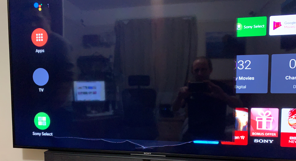
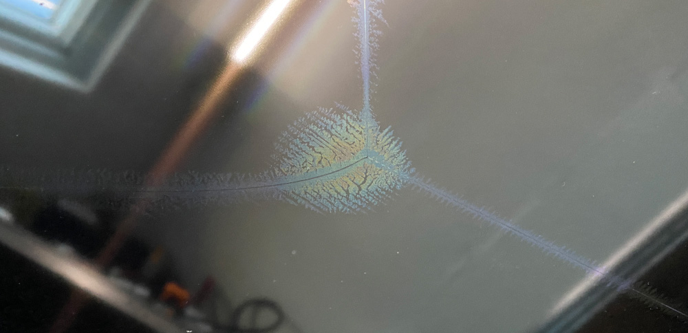
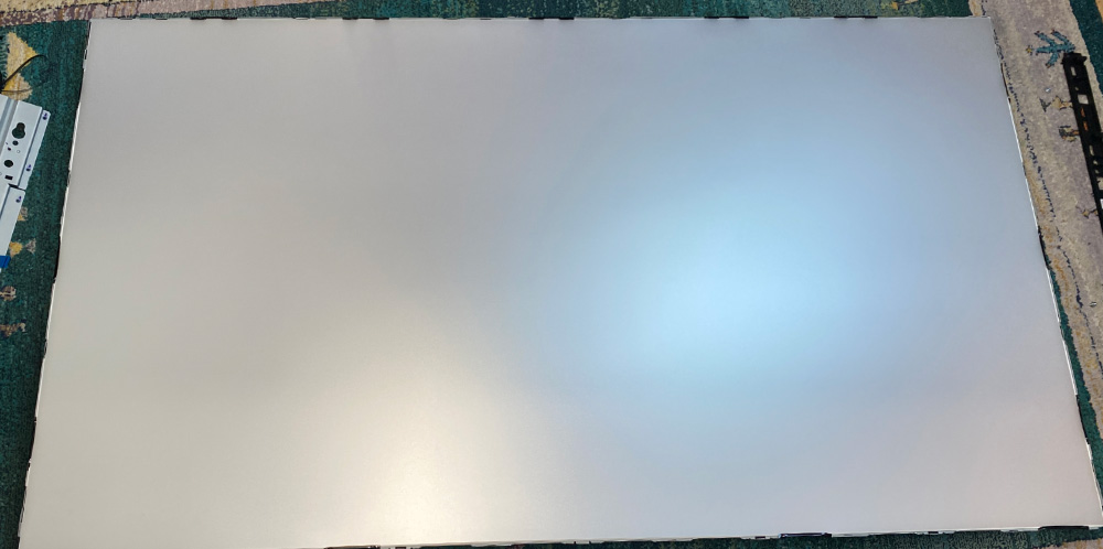
At first, we thought the only damage to the screen was only scuff marks which wiped off with some glass cleaner but after powering on the TV, I found the full extent of the damage with the centre part of the display not working and a large crack across the lower part of the screen as you can see on the photo below.
As the television was now dead and a replacement panel didn’t appear to be available to repair it, we decided to strip it down to see what you get inside a £1000 LED HDR 4K Ultra HD Smart TV before taking the bits to the local recycling centre.
The Teardown
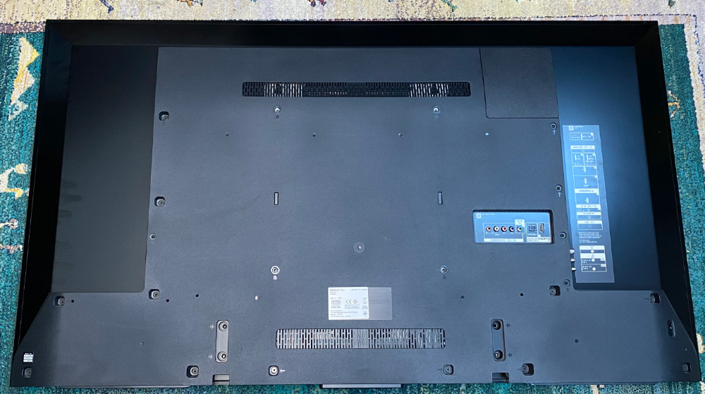
The back cover was held on with cross-head screws around the edges and middle.
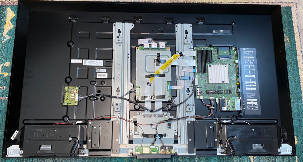
With the rear plastic cover removed it revealed the circuit boards and mounting brackets on the back of the TV. At the base of the TV are a pair of slimline speakers and between these are three small PCBs, one with an infrared receiver and the second with a WiFi module and antennas and a third with a single IC which we haven’t been able to establish what it does.
Above this is the display driver board and in the centre of the TV panel is a large PCB which is the LED backlight driver.
On the left of the TV is the power input board which uses a DC socket from an external 19V power supply, and this board has input filtering capacitors and inductors.
The right side holds the main input and processing circuit board which has a small RF input daughter board fitted into the lower edge.
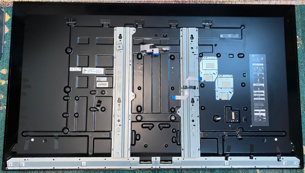
After removing the circuit boards and cables you are left with the display panel and wall mounting bars which are held together with several small screws. The edge of the screen has a plastic and metal bezel which is held on with more small screws. The display panel part number was: YD7S550DND01B A2187580A.
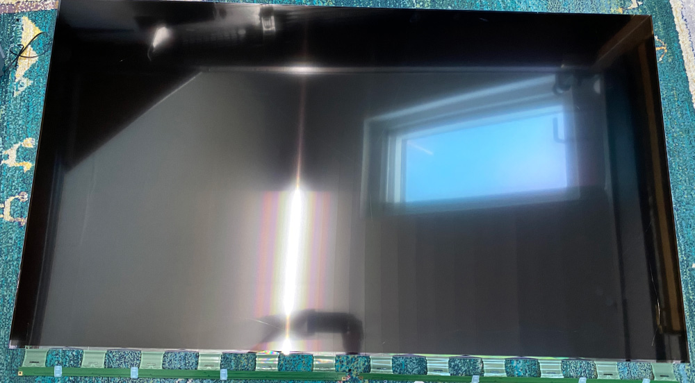
Removing these screws allows you to lift the LCD panel away which revealed the damage from the VR impact. The LCD panel has two long PCBs at the bottom which connect via flat flex to the screen and two connectors to connect to the display driver board.
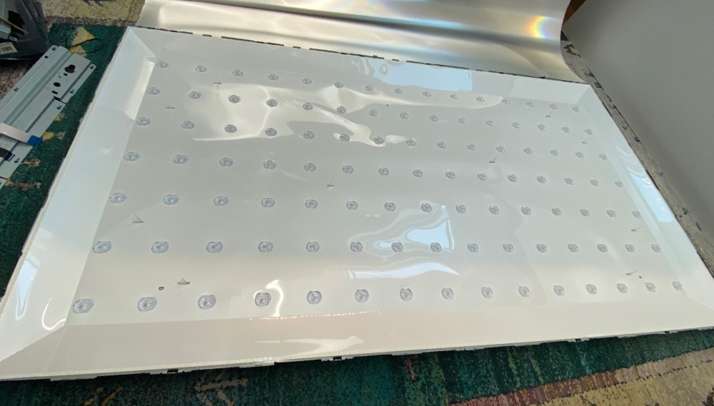
Under the LCD panel are several layers of light-diffusing material comprising of a Reflective Polarizer, Prism Sheet, Diffuser plate and Reflective sheet.
Under these are the backlight LEDs with a white reflective layer of plastic which is taped down along the edges.
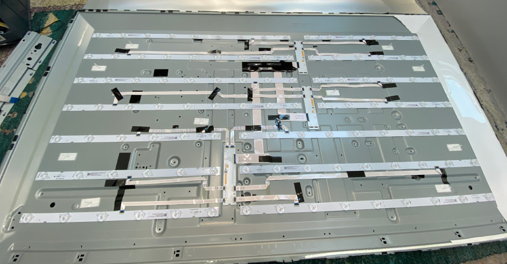
The LED strips are mounted onto aluminium strip PCBs and these are held to the metal chassis using double-sided tape.
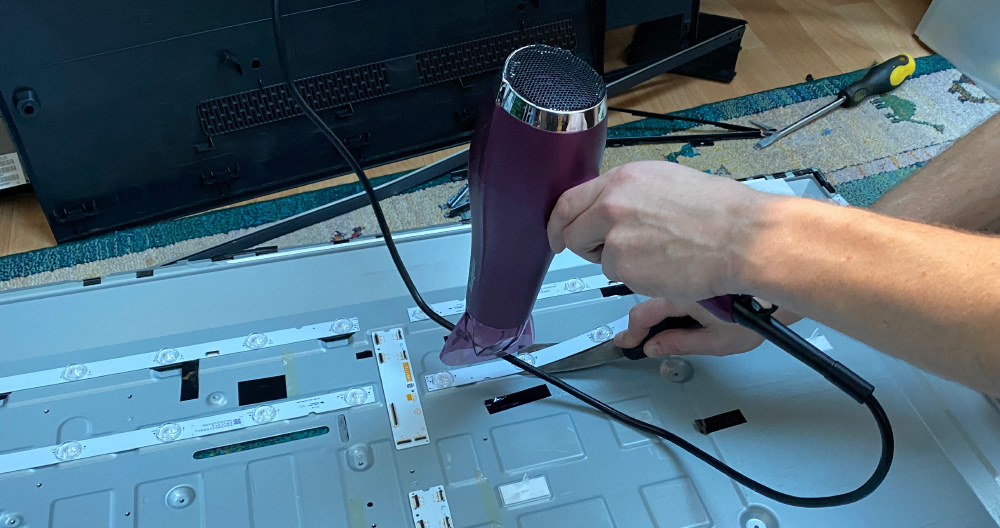
The glue holding the LED strips onto the back-metal panel was softened using a hair dryer and this allowed us to remove the LED strips from the TV.
Circuit Boards
All board locations listed below are when viewed from the back of the television.
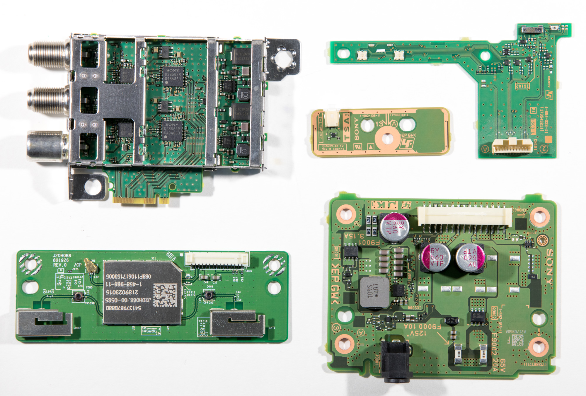
Power Input PCB
Located on the left side of the TV, this has a power input socket and power filtering and regulation components.
RF Input daughterboard PCB
The RF input PCB is located on the lower-right side of the TV and is connected to the main input and processing PCB via a header connector. There are a pair of RF input ICs marked Sony D2856ER
Wifi module and antenna PCB
This small PCB located at the bottom of the TV has a WiFi and Bluetooth module which is marked as J20H088 and is made by Foxconn
Infrared Receiver PCB
This small PCB located at the bottom of the TV has an infrared receiver module and also a small light sensor.
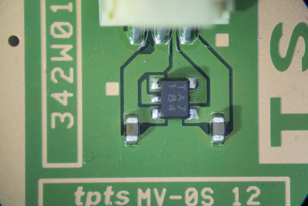
Unknown function PCB
This small PCB located at the bottom of the TV has a single 5-pin IC marked TA7 184 and two capacitors. I haven't been able to find any information about this chip or its function.
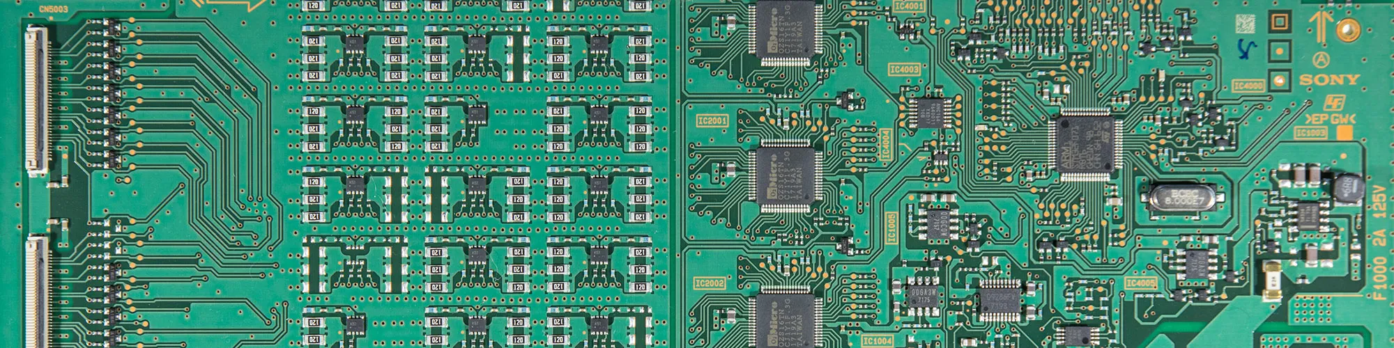
Display Driver PCB
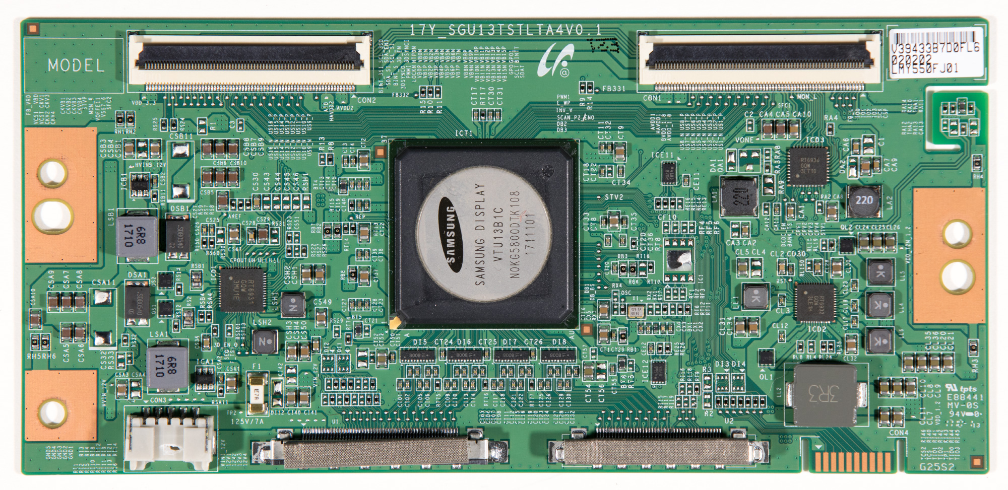
The display driver PCB is located at the bottom of the TV and has a Samsung VTU13B1C display controller IC which appears to be a commonly used 4K display driver on different brands of televisions.
LED Backlight Driver PCB
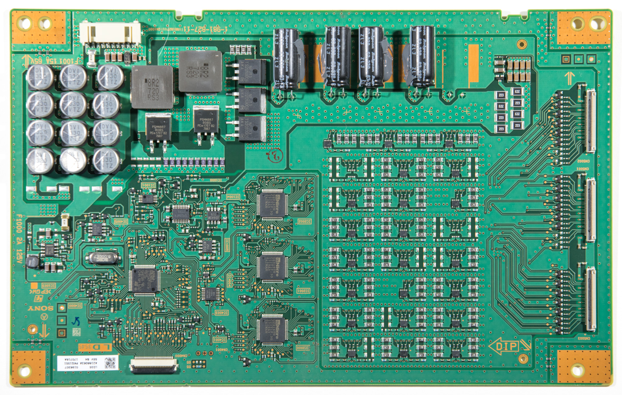
The LED backlight PCB is in the centre of the TV and contains driver ICs and power regulation for the LED backlight arrays which are connected by three flat flex cables. The main driver ICs are OZS16TN which are made by O2Micro International Ltd. The manufacturer doesn’t have any datasheets available for this IC. There is also an ARM STM32F071 microcontroller which is an ARM Cortex-M0 Access line MCU with 128 Kbytes Flash, 48 MHz CPU and CEC functions.
Main Processing and Input PCB
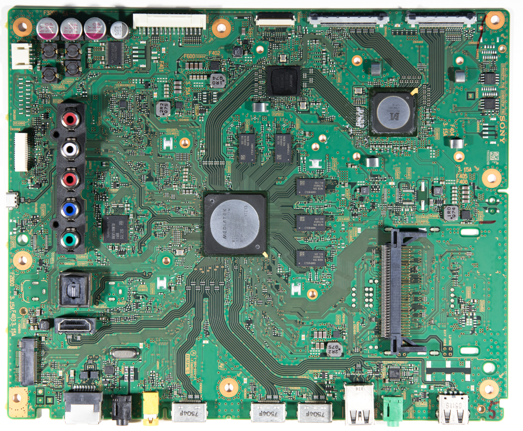
The main processing and input PCB contains the HDMI inputs and outputs and connects to the other circuit boards via ribbon cables and other higher-power connectors. The main processor is a Mediatek MT5832DG1U with a second processor marked MST7411FD
Reusing the LED strips
As we now have 14 aluminium-backed LED strips with 105 LEDs overall, we are planning to use some of these for lighting our CNC milling machine and lathe.
We have tested the LEDs using our current limited power supply and each LED illuminates at 12 Volts and 160mA which is approximately 2 watts for each LED.
The LEDs are connected in strips of three on the PCBs and so we can either create a current-limited 36 Volt power supply or cut the PCB traces on the PCBs and solder wires to the test points on each side of the LEDs to power them from a 12 Volt supply.

GIo
Interesting!
I have the same TV, the screen is ok, but I had a problem with mainboard.
I replaced it easily, but now the headphone jack and the USB 3.1 block is not working (So the PVR function :( )
Could it be some bad wire connection or the new mainboard is defective?
Keith
Hi Brian, is it possible to replace the LCD screen on a Sony Bravia KD 55XE9005? Thanks
Brian
Hi Keith, it should be possible to replace the screen if you can find one to buy. These sort of parts seem very difficult to find and order.
Anna Orlinski
Hi Brian I have 2 sony bravia tv’s both new the big one I think is around 55 or 60 has a pcb missing it was missing when I bought it so I bought a new Sony qled tv smaller but new the screen is smashed but all the parts are in it can I replace the missing board with the one from mine also could I add the Qled board to mine if so could you advise how I can do this ?
Kind regards Anna
Brian
Hi Anna
If the model numbers are the same you should be able to replace the missing PCB
warwick
Hi,
Excellent article. I have one of these and it is working, but won't boot. Is there any other reset to load the new flash, without the standard hold buttons whilst switching on?
Dirk van Leeuwen
Hi Brian, I have the same TV. Since a few days there is a horizontal black line about 12 cm above the botten. It must be possible to solve this problem with non conductive tape. What or where are the two connectors I have to check?
Thanks for your pdf file and your help in advance.
Regards Dirk.
Brian
Hi Dirk
Thank you for your comments, if there is a black line this is normally caused by a loose connector to the screen or a dead driver for that row. The best way to check is to carefully remove and reinstall all the connectors between the screen and controller boards to see if this solves the issue.
Glen Wilson
Hi Brian
I also have this TV, but unfortunatley it has the dreaded 4 blinking red lights boots and then shuts down.
Researched - it looks to be one of the LEDs on its way out sending an error signal which suts everything down.
It looks like most Sonys can have the same issue,but most sonys have a plug marked up as LCD ERR which this one appears not to.... typically, usually cutting this and grounding it as a work around will fix the issue for a time.
Would you have any idea how to tackle my issue?
Cheers Glen
tom
Hey glenn,i have the same issue. The service repair manual says tha 4 x blinking is either the mainboard or ldboard that is broken. They explain it how to measure it yourself.
Lars Fagerlind
I have the Sony KD-55XE9005, serial no. 6043082. It is dead. There are 19 V supply on all boards, byt no light or so anywhere. I had it to a repair shop, but they said that repair was too expensive, as the input and main processeo board is defect. Can you refer to a supplier to such a board? I have tried several suppliers, but this main board (YA03001AB) seems to be sold out everywhere.